AMD is gearing up for 7-nanometer CPUs and graphics cards
It's sampling "Zen 2" processors and has a 7-nanometer Radeon card in the lab.
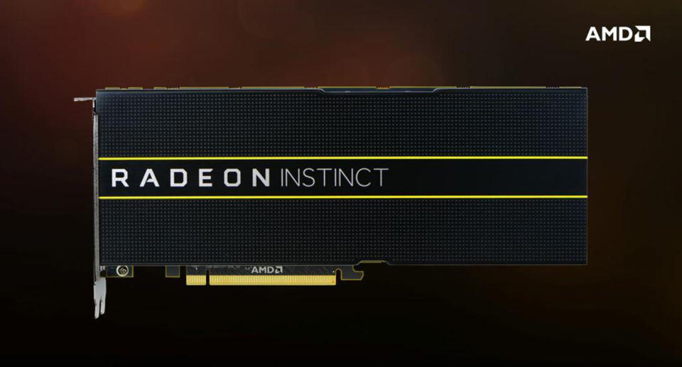
Intel recently told investors that its 10-nanometer "Cannon Lake" chips won't be ready until 2019, but by then, it might get leapfrogged by its PC arch-rival. AMD told investors that it's sampling next-gen Zen 2 processors with 7-nanometer tech in preparation for a launch in 2019. The company is also testing a Radeon Instinct machine learning graphics cards that use 7-nanometer Vega-based technology. The GPUs will be manufactured by TSMC, said AMD CEO Dr. Lisa Su, but the company will also use Global Foundries, presumably for processors and other products.
AMD recently launched its second-generation Zen chips, which uses 12-nanometer tech (technically a refined version of its current 14-nanometer tech). Zen 2, meanwhile, will move to a 7-nanometer manufacturing process. TSMC reportedly leads the race to develop that tech, which uses bleeding-edge deep and extreme ultraviolet lithography. It was a bit of a surprise that AMD would use TSMC for its graphics tech rather than GlobalFoundries, which AMD spun off itself in 2009.
If AMD can hit its targets, it'll put a lot of heat on Intel, which will only be introducing 10-nanometer tech by 2019. Intel has said that its tech is a "generation ahead" of 10-nanometer tech from other firms, but even if that's accurate, 7-nanometer chips would erase that gap. According to leaked slides, AMD's next-gen Vega graphics tech has double the bandwidth of its current GPUs.
AMD didn't say whether the 7-nanometer graphics tech that it's using for machine learning tech would come to gaming cards, but that seems a foregone conclusion -- it's just a question of when. Either way, things are finally going AMD's way, as it turned a $81 million profit this quarter on $1.65 billion of revenue, compared to a $33 million loss in the same quarter last year.
Update: The post previously said that AMD's second-gen Ryzen chips use 14-nanometer tech, but AMD and GlobalFoundries refer to it as 12-nanometer tech (technically, it's a refined version of the 14-nanometer process). It also said that 7-nanometer tech uses extreme ultraviolet (EUV) lithography, which it does, but TSMC's first version of it will use deep ultraviolet lithography, and the second generation chips will contain some EUV layers. The post has been updated with those changes.


